- 您现在的位置:买卖IC网 > Sheet目录2003 > LTC1400IS8 (Linear Technology)IC A/D CONV 12BIT W/SHTDN 8-SOIC
LTC1400
9
1400fa
APPLICATIO S I FOR ATIO
W
U
FREQUENCY (kHz)
0
40
80 100
140
180
20
60
120
160
200
AMPLITUDE
(dB)
1400 F05
0
–10
–20
–30
–40
–50
–60
–70
–80
–90
–100
–110
–120
fSAMPLE = 400kHz
fa = 99.512kHz
fb = 102.441kHz
fa fb
3fa
2fb – fa
2fa + fb
2fa – fb
2fb + fa
2fa
3fb
fa + fb
2fb
fb – fa
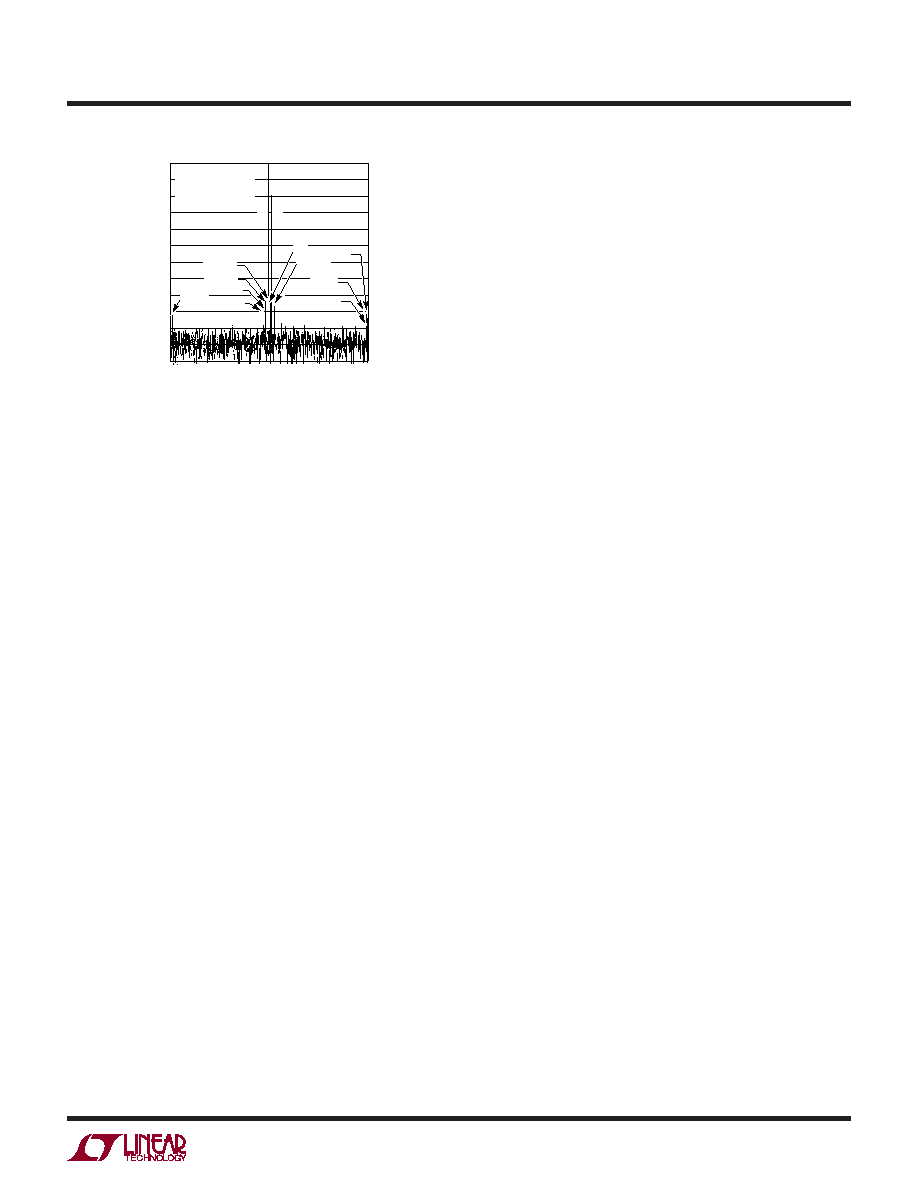
Figure 5. Intermodulation Distortion Plot in Bipolar Mode
Figure 5 shows the IMD performance at a 100kHz input.
Peak Harmonic or Spurious Noise
Thepeakharmonicorspuriousnoiseisthelargestspectral
component excluding the input signal and DC. This value
is expressed in decibels relative to the RMS value of a
full-scale input signal.
Full Power and Full Linear Bandwidth
The full power bandwidth is the input frequency at which
theamplitudeofthereconstructedfundamentalisreduced
by 3dB for a full-scale input signal.
The full linear bandwidth is the input frequency at which
the S/(N + D) has dropped to 68dB (11 effective bits). The
LTC1400 has been designed to optimize input bandwidth,
allowing the ADC to undersample input signals with fre-
quencies above the converter’s Nyquist Frequency. The
noise oor stays very low at high frequencies; S/(N +
D) becomes dominated by distortion at frequencies far
beyond Nyquist.
Driving the Analog Input
The analog input of the LTC1400 is easy to drive. It draws
only one small current spike while charging the sample-
and-hold capacitor at the end of a conversion. During
conversion, the analog input draws only a small leakage
current. The only requirement is that the amplier driv-
ing the analog input must settle after the small current
spike before the next conversion starts. Any op amp that
settles in 200ns to small load current transient will allow
maximum speed operation. If a slower op amp is used,
more settling time can be provided by increasing the time
between conversions. Suitable devices capable of driving
the ADC’s AIN input include the LT1360 and the LT1363
op amps.
LTC1400 comes with a built-in unipolar/bipolar detection
circuit. If VSS potential is forced below GND, the internal
circuitry will automatically switch to bipolar mode.
The following list is a summary of the op amps that are
suitable for driving the LTC1400, more detailed informa-
tion is available in the Linear Technology databooks or the
Linear Technology Website.
LT1215/LT1216: Dual and quad 23MHz, 50V/μs single
supply op amps. Single 5V to ±15V supplies, 6.6mA
specications, 90ns settling to 0.5LSB.
LT1223: 100MHz video current feedback amplier. ±5V
to ±15V supplies, 6mA supply current. Low distortion up
to and above 400kHz. Low noise. Good for AC applica-
tions.
LT1227: 140MHz video current feedback amplier. ±5V to
±15V supplies, 10mA supply current. Lowest distortion
at frequencies above 400kHz. Low noise. Best for AC
applications.
LT1229/LT1230: Dual and quad 100MHz current feedback
ampliers.±2Vto±15Vsupplies,6mAsupplycurrenteach
amplier. Low noise. Good AC specs.
LT1360: 37MHz voltage feedback amplier. ±5V to ±15V
supplies. 3.8mA supply current. Good AC and DC specs.
70ns settling to 0.5LSB.
LT1363: 50MHz, 450V/μs op amps. ±5V to ±15V supplies.
6.3mA supply current. Good AC and DC specs. 60ns
settling to 0.5LSB.
LT1364/LT1365:Dualandquad50MHz,450V/μsopamps.
±5V to ±15V supplies, 6.3mA supply current per amplier.
60ns settling to 0.5LSB.
Internal Reference
The LTC1400 has an on-chip, temperature compensated,
curvature corrected, bandgap reference, which is factory
发布紧急采购,3分钟左右您将得到回复。
相关PDF资料
LTC1401IS8#TRPBF
IC A/D CONV 12BIT W/SHTDN 8-SOIC
LTC1402IGN#TRPBF
IC ADC 12BIT 2.2MSPS SHDN 16SSOP
LTC1403AHMSE#TRPBF
IC ADC 14BIT 2.8MSPS DIFF 10MSOP
LTC1403AIMSE-1#TRPBF
IC ADC 14BIT 2.8MSPS DIFF 10MSOP
LTC1404IS8#TRPBF
IC A/D CONV 12BIT W/SHTDN 8-SOIC
LTC1405IGN#TRPBF
IC ADC 12BIT 5MSPS SAMPLE 28SSOP
LTC1406IGN#TRPBF
IC A/D CONV 8BIT SAMPLING 24SSOP
LTC1407AHMSE#PBF
IC ADC 14BIT 3MSPS 10-MSOP
相关代理商/技术参数
LTC1400IS8#PBF
功能描述:IC A/D CONV 12BIT W/SHTDN 8-SOIC RoHS:是 类别:集成电路 (IC) >> 数据采集 - 模数转换器 系列:- 标准包装:1 系列:microPOWER™ 位数:8 采样率(每秒):1M 数据接口:串行,SPI? 转换器数目:1 功率耗散(最大):- 电压电源:模拟和数字 工作温度:-40°C ~ 125°C 安装类型:表面贴装 封装/外壳:24-VFQFN 裸露焊盘 供应商设备封装:24-VQFN 裸露焊盘(4x4) 包装:Digi-Reel® 输入数目和类型:8 个单端,单极 产品目录页面:892 (CN2011-ZH PDF) 其它名称:296-25851-6
LTC1400IS8#TR
功能描述:IC ADC 12BIT 400KSPS SHTDN 8SOIC RoHS:否 类别:集成电路 (IC) >> 数据采集 - 模数转换器 系列:- 标准包装:1,000 系列:- 位数:16 采样率(每秒):45k 数据接口:串行 转换器数目:2 功率耗散(最大):315mW 电压电源:模拟和数字 工作温度:0°C ~ 70°C 安装类型:表面贴装 封装/外壳:28-SOIC(0.295",7.50mm 宽) 供应商设备封装:28-SOIC W 包装:带卷 (TR) 输入数目和类型:2 个单端,单极
LTC1400IS8#TRPBF
功能描述:IC A/D CONV 12BIT W/SHTDN 8-SOIC RoHS:是 类别:集成电路 (IC) >> 数据采集 - 模数转换器 系列:- 标准包装:1,000 系列:- 位数:16 采样率(每秒):45k 数据接口:串行 转换器数目:2 功率耗散(最大):315mW 电压电源:模拟和数字 工作温度:0°C ~ 70°C 安装类型:表面贴装 封装/外壳:28-SOIC(0.295",7.50mm 宽) 供应商设备封装:28-SOIC W 包装:带卷 (TR) 输入数目和类型:2 个单端,单极
LTC1400IS8PBF
制造商:Linear Technology 功能描述:ADC SAR 400ksps 12-Bit Serial SOIC8
LTC1401CS8
功能描述:IC A/D CONV 12BIT W/SHTDN 8-SOIC RoHS:否 类别:集成电路 (IC) >> 数据采集 - 模数转换器 系列:- 标准包装:2,500 系列:- 位数:16 采样率(每秒):15 数据接口:MICROWIRE?,串行,SPI? 转换器数目:1 功率耗散(最大):480µW 电压电源:单电源 工作温度:-40°C ~ 85°C 安装类型:表面贴装 封装/外壳:38-WFQFN 裸露焊盘 供应商设备封装:38-QFN(5x7) 包装:带卷 (TR) 输入数目和类型:16 个单端,双极;8 个差分,双极 配用:DC1011A-C-ND - BOARD DELTA SIGMA ADC LTC2494
LTC1401CS8#PBF
功能描述:IC A/D CONV 12BIT W/SHTDN 8-SOIC RoHS:是 类别:集成电路 (IC) >> 数据采集 - 模数转换器 系列:- 标准包装:1 系列:microPOWER™ 位数:8 采样率(每秒):1M 数据接口:串行,SPI? 转换器数目:1 功率耗散(最大):- 电压电源:模拟和数字 工作温度:-40°C ~ 125°C 安装类型:表面贴装 封装/外壳:24-VFQFN 裸露焊盘 供应商设备封装:24-VQFN 裸露焊盘(4x4) 包装:Digi-Reel® 输入数目和类型:8 个单端,单极 产品目录页面:892 (CN2011-ZH PDF) 其它名称:296-25851-6
LTC1401CS8#TR
功能描述:IC ADC 12BIT 200KSPS SHTDN 8SOIC RoHS:否 类别:集成电路 (IC) >> 数据采集 - 模数转换器 系列:- 标准包装:2,500 系列:- 位数:16 采样率(每秒):15 数据接口:MICROWIRE?,串行,SPI? 转换器数目:1 功率耗散(最大):480µW 电压电源:单电源 工作温度:-40°C ~ 85°C 安装类型:表面贴装 封装/外壳:38-WFQFN 裸露焊盘 供应商设备封装:38-QFN(5x7) 包装:带卷 (TR) 输入数目和类型:16 个单端,双极;8 个差分,双极 配用:DC1011A-C-ND - BOARD DELTA SIGMA ADC LTC2494
LTC1401CS8#TRPBF
功能描述:IC A/D CONV 12BIT W/SHTDN 8-SOIC RoHS:是 类别:集成电路 (IC) >> 数据采集 - 模数转换器 系列:- 标准包装:2,500 系列:- 位数:16 采样率(每秒):15 数据接口:MICROWIRE?,串行,SPI? 转换器数目:1 功率耗散(最大):480µW 电压电源:单电源 工作温度:-40°C ~ 85°C 安装类型:表面贴装 封装/外壳:38-WFQFN 裸露焊盘 供应商设备封装:38-QFN(5x7) 包装:带卷 (TR) 输入数目和类型:16 个单端,双极;8 个差分,双极 配用:DC1011A-C-ND - BOARD DELTA SIGMA ADC LTC2494